Foundry Solutions Overview
MDT offers a complete magnetic sensor (AMR, GMR and TMR) development and wafer production service including design,fabrication, and testing.
MDT’s magnetic sensor foundry has the capability to fabricate 6 inch (currently)/8 inch(in plan) wafers at 0.5-micron (μm).Unlike other wafer foundries in Mainland China, MDT’s foundry specializes in magnetic device wafer fabrication, providing professional service with the specialized equipment and experienced staff necessary for magnetic device development and wafer processing.
Design Service
As a full turn-key foundry service provider, MDT offers design and modeling services to complement the wafer foundry capabilities. MDT can assist with the design of your product, including mask design, modeling of magnetic devices, and process flow development.
MDT can provide full mask design and tape-out service. Once we receive your initial design CAD files, we can integrate alignment targets, metrology sites and customer specific test structures into the reticle layout, provide verification and final tape out before shipping the design file to the mask manufacturer. We can also integrate MEMS or magnetic thin film devices on top of existing IC circuitry in order to provide fully integrated devices.
Design file customer exchange formats: GDSII, DXF, DWG and CIF.
CAD Layout environment: Tanner Tools L-Edit.
Capable of transforming customer device designs GDSII files used for mask manufacture for 1X, Nikon 5X, ASML 5X reticles, including appropriate integrate alignment targets, metrology sites, and test structures.
Capable of integrating MEMS and magnetic layers onto CMOS, BiCMOS, TFT, and other integrated circuit wafers.
Capable of modelling various magnetic devices including sensors, MRAM, logic, etc. to aid the design and development of the manufacturing process..
Capable of customer specific test structure design, multi-physics FEA, Computation Fluid Dynamics, micromagnetic simulation, high-frequency analysis, Spice simulations.
Fabrication
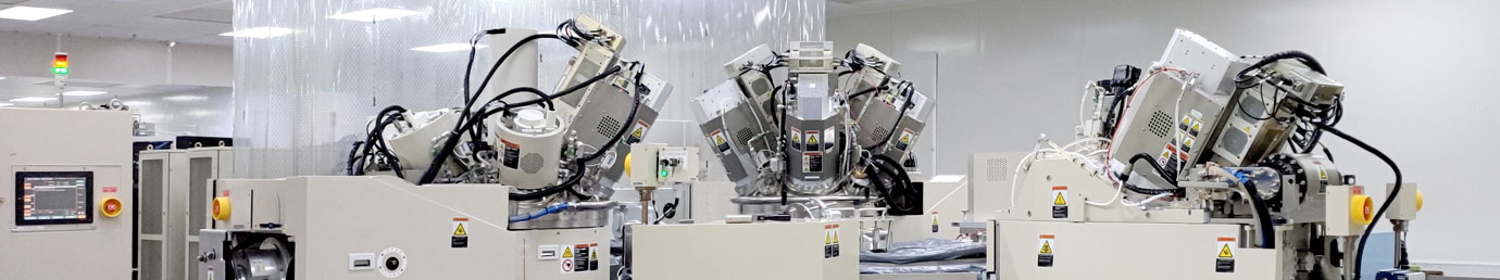
MDT can provide complete 6” wafer fabrication with proven technologies utilizing state of the art magnetic processing equipment; MDT will make great effort to continue optimizing the processes based on the customer’s requirements.
These offerings are supported by our strong manufacturing capability, cost-effective prototyping service, as well as a comprehensive suite of value-added services to help customers bring their products to market quickly and cost-effectively.
MDT’s processes and technologies are designed to meet the highest industry standards.
Wafer Probing / Testing Services
MDT's test facility provides customers with quick turn-around and strict quality control of wafer-level testing and the initial magnet setting. The wafer-level tests includes electric and magneto-resistive measurements at the controlled temperature.
Services offered include wafer probing, epoxy probe card building and repair as well as testing for contact IC card types.
magnetic sensor wafer-level dynamic range test (Rmax to Rmin) on EG6000 tester;
CWS wafer-level tester to provide a multi-axis magnetic field for 2-D magnetic bias (XY) for transfer curve and quasi-static measurements. The tester includes a high and low temperature sample evaluation ;
Capable of provide Multifunction probe card building and modify, also can be support the damaged probe card repair services.
Our wafer probing services include test program development as well as failure analysis and reliability testing.