Spintronics is the new science of computers and memory chips that are based on electron spin rather than (or in addition to) the charge (used in electronics). Spintronics is an exciting field that holds promise to build faster and more efficient computers and other devices.
Spintronicis: Fundamentals and applications;REVIEWS OF MODERN PHYSICS, VOLUME 76, APRIL 2004
Author: Igor Z ˇ utic, Jaroslav Fabian, S. Das Sarma;
1. Overview
Spintronics is a multidisciplinary field whose central theme is the active manipulation of spin degrees of freedom in solid-state systems. In this article the term spin stands for either the spin of a single electron s, which can be detected by its magnetic moment 2gmBs (mB is the Bohr magneton and g is the electron g factor, in a solid generally different from the free-electron value of g0=2.0023), or the average spin of an ensemble of electrons, manifested by magnetization. The control of spin is then a control of either the population and the phase of the spin of an ensemble of particles, or a coherent spin manipulation of a single or a few-spin system. The goal of spintronics is to understand the interaction between the particle spin and its solid-state environments and to make useful devices using the acquired knowledge. Fundamental studies of spintronics include investigations of spin transport in electronic materials, as well as of spin dynamics and spin relaxation. Typical questions that are posed are (a) what is an effective way to polarize a spin system? (b) how long is the system able toremember its spin orientation? and (c) how can spin be detected?
Generation of spin polarization usually means creating a nonequilibrium spin population. This can be achieved in several ways.
While traditionally spin has been oriented using optical techniques in which circularly polarized photons transfer their angular momenta to electrons, for device applications electrical spin injection is more desirable. In electrical spin injection a magnetic electrode is connected to the sample. When the current drives spin-polarized electrons from the electrode to the sample, nonequilibrium spin accumulates there. The rate of spin accumulation depends on spin relaxation, the process of bringing the accumulated spin population back to equilibrium. There are several mechanisms of spin relaxation, most involving spin-orbit coupling to provide the spin-dependent potential, in combination with momentum scattering to provide a randomizing force. Typical time scales for spin relaxation in electronic systems are measured in nanoseconds, while the range is from picoseconds to microseconds. Spin detection, also part of a generic spintronic scheme, typically relies on sensing the changes in the signals caused by the presence of nonequilibrium spin in the system.
The common goal in many spintronic devicesis to maximize the spin detection sensitivity to the point that it detects not the spin itself, but changes in the spin states.
2. History and background
(1)Spin-polarized transport and magnetoresistive effects
In a pioneering work, Mott (1936a, 1936b) provided a basis for our understanding of spin-polarized transport. Mott sought an explanation for an unusual behavior of resistance in ferromagnetic metals. He realized that at sufficiently low temperatures, where magnon scattering becomes vanishingly small, electrons of majority and minority spin, with magnetic moment parallel and antiparallel to the magnetization of a ferromagnet, respectively, do not mix in the scattering processes. The conductivity can then be expressed as the sum of two independent and unequal parts for two different spin projections—the current in ferromagnets is spin polarized.
Tunneling measurements played a key role in early experimental work on spin-polarized transport. Studying N/F/N junctions, where N was a nonmagnetic metal and F was an Eu-based ferromagnetic semiconductor (Kasuya and Yanase, 1968; Nagaev, 1983),revealed that I-V curves could be modified by an applied magnetic field (Esaki et al., 1967) and now show potential for developing a solid-state spin filter. When unpolarized current is passed across a ferromagnetic semiconductor, the current becomes spin-polarized (Moodera et al., 1988; Hao et al., 1990).
(2) Spin injection and optical orientation
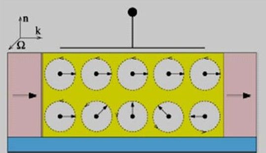
Many materials in their ferromagnetic state can have a substantial degree of equilibrium carrier spin polarization. However, as illustrated in Fig. 1, this alone is usually not sufficient for spintronic applications, which typically require current flow and/or manipulation of the nonequilibrium spin (polarization). The importance of generating nonequilibrium spin is not limited to device applications; it can also be used as a sensitive spectroscopic tool to study a wide variety of fundamental properties ranging from spin-orbit and hyperfine interactions (Meier and Zakharchenya, 1984) to the pairing symmetry of high-temperature superconductors (Vas’ko et al., 1997; Wei et al., 1999; Tsuei and Kirtley, 2000; Ngai et al., 2004) and the creation of spin-polarized beams to measure parity violation in high-energy physics (Pierce and Celotta, 1984).

Fig.1 spin field-effect transistor (SFET).
3. Recent Progress
Until recently, the spin of the electron was ignored in mainstream charge-based electronics. A technology has emerged called spintronics (spin transport electronics or spin based electronics), where it is not the electron charge but the electron spin that carries information, and this offers opportunities for a new generation of devices combining standard microelectronics with spin-dependent effects that arise from the interaction between spin of the carrier and the magnetic properties of the material. Traditional approaches to using spin are based on the alignment of a spin (either “up” or “down”) relative to a reference (an applied magnetic field or magnetization orientation of the ferromagnetic film). Device operations then proceed with some quantity (electrical current) that depends in a predictable way on the degree of alignment. Adding the spin degree of freedom to conventional semiconductor charge-based electronics or using the spin degree of freedom alone will add substantially more capability and performance to electronic products. The advantages of these new devices would be nonvolatility, increased data processing speed, decreased electric power consumption, and increased integration densities compared with conventional semiconductor devices.
Major challenges in this field of spintronics that are addressed by experiment and theory include the optimization of electron spin lifetimes, the detection of spin coherence in nanoscale structures, transport of spin-polarized carriers across relevant length scales and heterointerfaces, and the manipulation of both electron and nuclear spins on sufficiently fast time scales. In response, recent experiments suggest that the storage time of quantum information encoded in electron spins may be extended through their strong interplay with nuclear spins in the solid state. Moreover, optical methods for spin injection, detection, and manipulation have been developed that exploit the ability to precisely engineer the coupling between electron spin and optical photons. It is envisioned that the merging of electronics, photonics, and magnetic will ultimately lead to new spin-based multifunctional devices such as spin-FET (field effect transistor), spin-LED (light-emitting diode), spin RTD (resonant tunneling device), optical switches operating at terahertz frequency, modulators, encoders, decoders, and quantum bits for quantum computation and communication. The success of these ventures depends on a deeper understanding of fundamental spin interactions in solid state materials as well as the roles of dimensionality, defects, and semiconductor band structure in modifying these dynamics. If we can understand and control the spin degree of freedom in semiconductors, semiconductor hetero structures, and ferromagnets, the potential for high-performance spinbased electronics will be excellent.
4. Theories of spintronics (Generation of spin polarization)
Spin polarization not only of electrons, but also of holes, nuclei, and excitations can be defined as PX=Xs /X, the ratio of the difference Xs =Xλ-X-λ, and the sum X= Xλ+ X-λ of the spin-resolved λ components for a particular quantity X. To avoid ambiguity as to what precisely is meant by spin polarization, both the choice of the spin-resolved components and the relevant physical quantity X need to be specified. Conventionally, λ is taken to be ↑ or + (numerical value +1) for spin up, and ↓ or - (numerical value -1) for spin down, with respect to the chosen axis of quantization. In ferromagnetic metals it is customary to refer to ↑ (↓) as carriers with magnetic moment parallel (antiparallel) to the magnetization or, equivalently, as carriers with majority or minority spin (Tedrow and Meservey, 1973). In semiconductors the terms majority and minority usually refer to relative populations of the carriers while ↑ or + and ↓ or -correspond to the quantum numbers mj with respect to the z axis taken along the direction of the light propagation or along the applied magnetic field (Meier and Zakharchenya, 1984; Jonker et al., 2003). It is important to emphasize that both the magnitude and the sign of the spin polarization in Eq. (3) depend on the choice of X, relevant to the detection technique employed, say optical vs transport and bulk vs surface measurements (Mazin, 1999; Jonker et al., 2003). Even in the same homogeneous material the measured PX can vary for different X, and it is crucial to identify which physical quantity—charge current, carrier density, conductivity, or the density of states—is being measured experimentally.
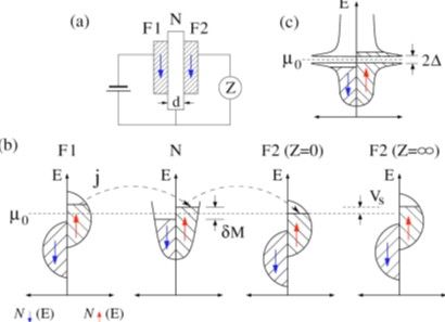
The spin polarization of electrical current or carrier density, generated in a nonmagnetic region, is typically used to describe the efficiency of electrical spin injection. Silsbee (1980) suggested that the nonequilibrium density polarization in the N region, or equivalently the nonequilibrium magnetization, acts as the source of spin electromotive force (emf) and produces a measurable ‘‘spin-coupled’’ voltage Vs∝δM. Using this concept, also referred to as spin-charge coupling, Silsbee (1980) proposed a detection technique consisting of two ferromagnets F1 and F2 (see Fig. 2) separated by a nonmagnetic region. F1 serves as the spin injector (spin aligner) and F2 as the spin detector. This could be called the polarizer-analyzer method, the optical counterpart of the transmission of light through two optical linear polarizers. From Fig. 2 it follows that the reversal of the magnetization direction in one of the ferromagnets would lead either to Vs→-Vs , in an open circuit (in the limit of large impedance Z), or to the reversal of charge current j→-j, in a short circuit (at small Z), a consequence of Silsbee-Johnson spin-charge coupling (Silsbee, 1980; Johnson and Silsbee, 1987, 1988a).Correspondingly, spin injection could be detected through the spin accumulation signal as either a voltage or a resistance change when the magnetizations in F1 and F2 are changed from parallel to antiparallel alignment.

Fig.2 Spin injection, spin accumulation, and spin detection
5. Spintronic Devices and Application
Spin filters
Solid-state spin filtering was first realized in N/F/N tunneling. It was shown by Esaki et al. (1976) that magnetic tunneling through (ferro)magnetic semiconductor Eu chalcogenides (von Molna´ r and Methfess, 1967; Kasuya and Yanase, 1968; Nagaev, 1983), such as EuSe and EuS,could be modified by an applied magnetic field. The change in I-V curves in the N/F/N structure, where N is a normal metal and F is a ferromagnet, was explained by the influence of the magnetic field on the height of the barrier formed at the N/F interface (for EuSe, the barrier height was lowered by 25% at 2 T). The large spin splitting of the Eu chalcogenides was subsequently employed in the absence of applied field with EuS (Moodera et al., 1988), and nearly 100% spin polarization was reached at B=1.2 T with EuSe (Moodera et al., 1993). These spin-filtering properties of the Eu chalcogenides, used together with one-electron quantum dots, were proposed as the basis for a method to convert single spin into single charge measurements and provide an important ingredient in realizing a quantum computer (DiVincenzo, 1999); Zeeman splitting in semiconductor heterostructures and superlattices (enhanced by large g factors; Egues, 1998; Guo et al., 2001), in quantum dots (Recher et al.,2000; Deshmukh and Ralph, 2002; Borda et al., 2003), and nanocrystals (Efros et al., 2001) provide effective spin filtering and spin-polarized currents. Predicted quantum size effects and resonance tunneling (Duke, 1969, p. 79) also have their spin-dependent counterparts. The structures studied are typically double-barrier resonant tunneling diodes (for an early spin-unpolarized study see Tsu and Esaki, 1973), either with Zeeman splitting or using ferromagnetic materials, in which spinfiltering can be tuned by an applied bias.
Several other realizations of spin filtering have been investigated, relying on spin-orbit coupling or hot-electron transport across ferromagnetic regions, discussed in more detail in Sec. IV.E.3. A choice of particular atomically ordered F/Sm interfaces was suggested to give a strong spin-filtering effect (Kirczenow, 2001), limited by the spin-orbit coupling and interfacial spin-flip scattering.
Spin diodes
Spin diodes are inhomogeneous two-terminal devices whose electronic or optical properties depend on the spin polarization of the carriers. Such devices were envisaged long before the emergence of spintronics. Solomon (1976), for example, proposed and demonstrated a silicon p-n junction whose current was modified by changing the spin polarization of the recombination centers. In a magnetic field both the mobile carriers and the recombination centers have an equilibrium spin polarization due to the Zeeman splitting.
The current in a p-n junction depends on the recombination rate, which, in turn, depends on the relative orientation of the spin of the carriers and the centers (Lepine, 1972). The trick to modifying the current is to decrease (even saturate) the spin polarization of either the electrons or the centers by electron spin resonance. Indeed, Solomon (1976) found a variation of '0.01% of the saturation current at small biases where recombination in the space-charge region dominates. Similar experiments could be used to detect nonequilibrium spin due to (potential) spin injection in Si, where optical methods are ineffective, but also in other semiconductors where electrical detection would be desirable.
Several spin diodes have recently been proposed or demonstrated with the goal of either maximizing the sensitivity of the I-V characteristics to spin and magnetic field, or facilitating spin injection and its detection through semiconductor interfaces comprising a magnetic semiconductor as the injector. Magnetic tunneling diodes have been used for spin injection from a ferromagnetic to a nonmagnetic semiconductor,p-n heterostructures have combined Cr- or Eu-based ferromagnetic semiconductors and InSb (Viglin et al., 1997; Osipov et al., 1998). Spin light-emitting diodes were employed for injecting and detecting spins in semiconductors, while resonant tunneling diodes have been demonstrated as effective spin injectors and spin filters. A magnetic unipolar diode has been proposed by Flatte´ and Vignale (2001) to simulate the working of ordinary diodes, but with homogeneous monopolar doping (either donors or acceptors, not both). The role of inhomogeneous doping in the p-n junction is played by the inhomogeneous spin splitting of the carrier band, with the spin-up and spin-down carriers playing roles similar to those of the electrons and holes in bipolar diodes. Si-based p-i-n diode sandwiched between two ferromagnetic metals was suggestedto allow controlling the device performance by an externally applied magnetic field (Dugaev et al., 2003).
Spin transisitors
Various spin transistors that contain metallic (and insulating) regions have been proposed (Johnson, 1993a;You and Bader, 2000; Bauer et al., 2003; Zvezdin et al.,2003). There is also a large category of spin single electron transistors, first realized by Ono et al.(1996), and later investigated by Barnas´ and Fert (1998); Korotkov and Safarov (1999); Ciorga et al. (2002); and Martinek et al. (2002).
Spin single-electron transistors can be viewed as an extension of magnetic tunneling to double tunnel junctions, where the Coulomb blockade becomes important (Takahashi and Maekawa, 1998). For a review of spin single-electron transistors see Maekawa et al.(2002).
(1) Spin field-effect transistors
The magnetic bipolar transistor (MBT) is a bipolar transistor with spin-split carrier bands and, in general, an injected spin source (Fabian et al., 2002b, 2004; Fabian and Z ˇ utic´, 2004). A related device structure was already proposed by Gregg et al. (1997) in a push for silicon-based spintronics. In this proposal (also called SPICE for spin-polarized injection current emitter) the semiconductors have no equilibrium spin, while the spin source is provided by a ferromagnetic spin injector attached to the emitter, and another ferromagnetic metal, a spin detector, is attached to the base/collector junction to modulate the current flow. In both configurations the aim is to control current amplification by spin and magnetic field.
(2) Magnetic bipolar transistor
The magnetic bipolar transistor (MBT) is a bipolar transistor with spin-split carrier bands and, in general, an injected spin source (Fabian et al., 2002b, 2004; Fabian and Z ˇ utic´, 2004). A related device structure was already proposed by Gregg et al. (1997) in a push for silicon-based spintronics. In this proposal (also called SPICE for spin-polarized injection current emitter) the semiconductors have no equilibrium spin, while the spin source is provided by a ferromagnetic spin injector attached to the emitter, and another ferromagnetic metal, a spin detector, is attached to the base/collector junction to modulate the current flow. In both configurations the aim is to control current amplification by spin and magnetic field.
(3) Hot-electron spin transistors
Spin transistors that rely on transport of hot (nonthermalized) carriers have the potential of serving several different purposes. On the one hand, they could be used as a diagnostic tool to characterize spin- and energydependent interfacial properties, scattering processes, and electronic structure, relevant to spintronic devices. On the other hand, hot-electron transistors are also of interest for their ability to sense magnetic fields, their possible memory applications, and their potential as a source of ballistic hot-electron spin injection. There are two representative examples, a spin-valve transistor and a magnetic tunneling transistor.
Future studies of hot-electron spin transistors are expected to result in increased spin injection even at room temperatures and to utilize other semiconductor collectors.
It would be particularly desirable to demonstrate hot-electron spin injection in Si and facilitate an integration with the complementary metal-oxide semiconductor technology.


